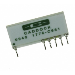
TA33-20KF vs TA33-140RFD
| Part Number |

|

|
| Category | Resistor Networks, Arrays | Resistor Networks, Arrays |
| Manufacturer | Vishay Sfernice | Vishay Sfernice |
| Description | SFERNICE THIN FILMS | SFERNICE THIN FILMS |
| Package | Tray | Tray |
| Series | - | - |
| Operating Temperature | - | - |
| Mounting Type | - | - |
| Package / Case | - | - |
| Supplier Device Package | - | - |
| Applications | - | - |
| Tolerance | - | - |
| Temperature Coefficient | - | - |
| Size / Dimension | - | - |
| Resistance (Ohms) | - | - |
| Height - Seated (Max) | - | - |
| Circuit Type | - | - |
| Number of Resistors | - | - |
| Number of Pins | - | - |
| Power Per Element | - | - |
| Resistor Matching Ratio | - | - |
| Resistor-Ratio-Drift | - | - |

-
1. How to reduce network resistance?
The main methods for reducing network resistance include the following:
Improving the power factor of users: By reducing the reactive power transmitted by the line, the network resistance can be effectively reduced. This can be achieved by installing a reactive power compensation device.
Adding a reactive power compensation device: By adding a reactive power compensation device, the network energy loss can be reduced, thereby reducing the network resistance.
Implement economic distribution of power in a closed network: By reasonably distributing power and avoiding local overload, network resistance can be reduced.
Appropriately improve the operation level of the power grid: By optimizing the operation mode of the power grid, the efficiency of the power grid can be improved, thereby reducing network resistance.
Organize the economic operation of transformers: Reasonably arrange the operation mode of transformers to avoid overload, which can effectively reduce network resistance.
Adjust the user's load curve: By adjusting the user's load curve to avoid overload during peak hours, network resistance can be reduced.
-
2. What is an array in a circuit?
Types of arrays
Gate array: The gate array is a motherboard with basic logic gates formed on the silicon wafer provided by semiconductor manufacturers. Users can wire on the motherboard according to their needs to form the required circuit. This chip is semi-customized and is suitable for occasions that require specific functions.
PLA (Programmable Logic Array): PLA is a variant of ROM. Its storage unit body and address decoder are both user-programmable. It is suitable for occasions that require flexible configuration of logic functions.
PAL (Programmable Array Logic): PAL is also a variant of ROM. Its storage unit body is not programmable, but the address decoder is user-programmable. It is suitable for occasions that require partial programmable logic.
GAL (General Array Logic): GAL is more powerful than PLA and PAL, and is suitable for occasions that require more complex logic functions.
PGA (Programmable Gate Array): PGA is an array logic circuit with strong logic functions. Users can interconnect the gate circuits in the gate array as needed to achieve the required logic functions.
PMA (Programmable Macrocell Array): PMA is more powerful than PGA and has a higher degree of integration. It is suitable for occasions that require higher performance and complex logic.
PLD (Programmable Logic Device): PLD is a collective name for array logic circuits other than RAM, and is suitable for occasions that require flexible configuration of logic functions.
-
3. What is a SIP resistor network?
SIP resistor network usually refers to a resistor network using SIP (System-in-Package) technology. SIP technology is a system-in-package technology that packages multiple electronic components with different functions (including active and passive components) in a standard package to form a system or subsystem. Specifically, the SIP resistor network integrates multiple resistors and other electronic components in a package to achieve specific circuit functions.
Definition and application of SIP technology
SIP (System-in-Package) technology is to package multiple active electronic components with different functions and passive devices (such as resistors, capacitors, etc.) in a standard package to form a system or subsystem. This technology can significantly improve the integration of equipment, reduce the number of components, thereby reducing the volume and cost of the system, while improving the reliability and performance of the system. -
4. What is an array in a semiconductor?
The array in a semiconductor mainly refers to a memory cell array. The memory cell array is the core part of a semiconductor memory, which is composed of a large number of memory cells arranged in a certain pattern. Each memory cell can store one or more bits of data.
Structure and function of memory cell array
The memory cell array is a key component of semiconductor memory, which specifically includes the following parts:
Address decoder: translates the address signal into the selection signal of the corresponding memory cell, and cooperates with the read/write circuit to complete the read/write operation.
Read/write circuit: includes read amplifier and write circuit, used to complete read/write operation.
Control logic: determines the read/write operation of the chip.

