Renesas Electronics America Inc RJK03P9DPA-00#J5A

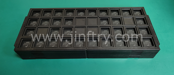
The picture is for reference only, please refer to the product specification
- RJK03P9DPA-00#J5A
- Renesas Electronics America Inc
- POWER, N-CHANNEL MOSFET
- Transistors - FETs, MOSFETs - Arrays
- RJK03P9DPA-00#J5A Datasheet
- 8-WFDFN Exposed Pad
- Bulk
-
 Lead free / RoHS Compliant
 - 1635
- Spot Inventory / Athorized Dstributor / Factory Excess Stock
- 1 year quality assurance 》
- Click to get rates


What is RJK03P9DPA-00#J5A
Renesas Electronics America Inc Part Number RJK03P9DPA-00#J5A(Transistors - FETs, MOSFETs - Arrays), developed and manufactured by Renesas Electronics America Inc, distributed globally by Jinftry. We distribute various electronic components from world-renowned brands and provide one-stop services, making us a trusted global electronic component distributor.
RJK03P9DPA-00#J5A is one of the part numbers distributed by Jinftry, and you can learn about its specifications/configurations, package/case, Datasheet, and other information here. Electronic components are affected by supply and demand, and prices fluctuate frequently. If you have a demand, please do not hesitate to send us an RFQ or email us immediately [email protected] Please inquire about the real-time unit price, Data Code, Lead time, payment terms, and any other information you would like to know. We will do our best to provide you with a quotation and reply as soon as possible.
RJK03P9DPA-00#J5A Specifications
- Part NumberRJK03P9DPA-00#J5A
- CategoryTransistors - FETs, MOSFETs - Arrays
- ManufacturerRenesas Electronics America Inc
- DescriptionPOWER, N-CHANNEL MOSFET
- PackageBulk
- Series-
- Operating Temperature150°C (TJ)
- Mounting TypeSurface Mount
- Package / Case8-WFDFN Exposed Pad
- Supplier Device Package8-WPAK
- Power - Max15W, 35W
- FET Type2 N-Channel (Half Bridge)
- FET FeatureLogic Level Gate, 4.5V Drive
- Drain to Source Voltage (Vdss)30V
- Current - Continuous Drain (Id) @ 25°C20A, 50A
- Rds On (Max) @ Id, Vgs7mOhm @ 10A, 10V
- Vgs(th) (Max) @ Id-
- Gate Charge (Qg) (Max) @ Vgs7.7nC @ 4.5V
- Input Capacitance (Ciss) (Max) @ Vds1660pF @ 10V
Application of RJK03P9DPA-00#J5A
RJK03P9DPA-00#J5A Datasheet
RJK03P9DPA-00#J5A Datasheet , Bulk,150°C (TJ),Surface Mount,8-WFDFN Exposed Pad,8-WPAK,15W, 35W,2 N-Channel (Half Bridge),Logic Level Gate, 4.5V Drive,30V,20A, 50A,7mOhm @ 10A, 10V,7.7nC @ 4.5V,1660pF @ 10V
RJK03P9DPA-00#J5A Classification
Transistors - FETs, MOSFETs - Arrays
FAQ about Transistors - FETs, MOSFETs - Arrays
-
1. What is the difference between transistors, FETs and MOSFETs?
The main differences between transistors, FETs and MOSFETs are their structure, working principle and application scenarios.
Transistor
A transistor is a three-terminal semiconductor device used to switch or amplify signals. It is divided into two main types: bipolar junction transistor (BJT) and field effect transistor (FET).
BJT: It consists of three layers of alternating P-type and N-type semiconductor materials, and uses two types of charge carriers (electrons and holes). It controls the collector current through the base current, with high gain but low input impedance.
FET: Including JFET and MOSFET, it uses electric fields to control charge carriers in semiconductor materials. FET is a unipolar transistor involving single-carrier operation.
FET (Field-Effect Transistor)
FET is a transistor that uses electric fields to control charge carriers in semiconductor materials. It is divided into JFET and MOSFET.
JFET: The simplest field effect transistor, which uses gate voltage to control the current between the drain and source. It is divided into two types, N-channel and P-channel, with high input impedance and low noise characteristics.
MOSFET: A four-terminal semiconductor field-effect transistor that controls the current between the source and drain through the gate voltage. MOSFET has high input impedance and is widely used in power amplifiers and switches, as well as embedded system design.
MOSFET (Metal-Oxide-Semiconductor Field-Effect Transistor)
MOSFET is a type of FET with four terminals: source, gate, drain, and body (or substrate). The body of the MOSFET is usually connected to the source terminal, making it appear as a three-terminal device in the circuit diagram. Due to its high input impedance, MOSFET plays an important role in integrated circuits, mainly used in power amplifiers and switches, and occupies an important position in embedded system design.
-
2. What is MOSFET and how does it work?
MOSFET (Metal-Oxide-Semiconductor Field-Effect Transistor), that is, metal-oxide-semiconductor field effect transistor, is a transistor that uses electric field effect to control conduction and shutdown. MOSFET controls the flow of current between the source and drain by applying voltage to the gate. Its working principle is as follows:
Working principle:
When a positive voltage is applied to the gate, the electric field causes the impurities in the substrate to form an "open" n-type or p-type conductive area, i.e., a channel, between the gate and the substrate. A capacitor is formed between the oxide layer above the channel and the gate, called the gate capacitance. When the channel conductive area extends to the source and drain, the MOSFET is in the on state. In the on state, the voltage difference between the source and the drain drives the current to flow through the conductive area.
When a negative voltage is applied to the gate, the channel on the substrate shrinks, the conductivity weakens, and the current between the source and the drain decreases. When the gate voltage continues to decrease, the channel eventually disappears, the MOSFET is in the off state, there is no conductive path between the source and the drain, and the MOSFET is in a high-resistance state.
-
3. Is MOSFET a transistor?
MOSFET is a type of transistor. MOSFET (Metal-Oxide-Semiconductor Field-Effect Transistor) is a metal oxide semiconductor field effect transistor, which is a type of field effect transistor.
Basic concepts and characteristics of MOSFET
MOSFET is an insulated gate field effect transistor that mainly controls the conductive channel between the source and the drain through the gate voltage. Its working principle is to apply voltage to the gate to form an electric field, thereby controlling the charge distribution on the surface of the semiconductor and thus controlling the flow of current. MOSFET has the advantages of high input impedance, low noise, and good frequency characteristics, and is widely used in analog circuits and digital circuits.
We are a professional PCB manufacturer who offers comprehensive PCB manufacturing services including: professional Ceramic PCB HDI PCB Heavy Copper PCB High-TG PCB High Speed PCB High Frequency PCB Metal Core PCB PCB fabrication and PCB assembly, providing fast turnaround prototypes for high-end products.


• Prompt Responsiveness
• Guaranteed Quality
• Global Access
• Competitive Market Price
• One-Stop support services of supply chain
Jinftry, Your most trustworthy component supplier, welcome to send us the inquiry, thank you!
Do you have any questions about RJK03P9DPA-00#J5A ?
Feel free to contact us:
RJK03P9DPA-00#J5A Related Products
-Z-E1-AZ 4795953")
N-CHANNEL POWER MOSFET

60V, 30A, DUAL N-CHANNEL POWER M
N-CHANNEL MOSFET

POWER, N-CHANNEL MOSFET


5A, 60V, N-CHANNEL MOSFET
-Z-E1-AZ 4795953")
N-CHANNEL POWER MOSFET SWITCHING