ADRF5141 Data Sheet, Functional Utilization, and Alternatives
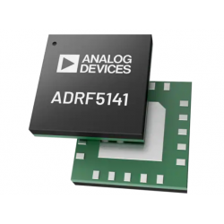
ADI ADRF5141 High Power Transmit and Receive Switch IC
ADRF5141 DataSheet, Functional Application Chip models of the same series include:
ADRF5130-EVALZ , ADRF5130BCPZ , ADRF5130BCPZ-R7 ..
ADI's ADRF5141 High Power Transmit and Receive Switch IC is a 50ΩΩ reflective SPDT switch IC fabricated on a silicon process. These switch ICs are designed for transmit and receive applications with an integrated power limiter on the receive path. The ADRF5141 switch IC operates in the 6GHz-12GHz frequency range. These high-power switching ICs draw a low 13µA on the 3.3V positive supply and 360µA on the -3.3V negative supply. The ADRF5141 switch IC uses complementary metal-oxide-semiconductor/low voltage transistor-to-transistor logic compatible controls. These switch ICs require no additional driver circuitry, making them ideal for replacing GaN and PIN diode-based switches.
The ADRF5141 switch IC features fast 50ns switching times and <10ns fast response and recovery times. These switch ICs are available in a 20-pin, 3.0mm x 3.0mm, land grid array package. The ADRF5141 high power switching IC is RoHS compliant and operates over the -40°C to 105°C temperature range. Typical applications include electronic countermeasures, microcommunications, and radar.
characteristic
High power transmit and receive switches with integrated power limiter on the receive path.
Frequency range: 6GHz--12GHz
Reflective 50Ω design
Dual power supply, no low frequency spurious
Low insertion loss:
TX to ANT:
Frequency range: 0.9dB (8GHz--11GHz)
ANT to RX:
Frequency range: 1.4dB (8GHz--11GHz)
High isolation:
TX to RX: 55dB (typical value, when TX is selected)
High power handling capability (TCASE=50°C)
TX input:
Pulse 40dBm, >100ns pulse width (15% duty cycle
)
ANT input:
Pulse 40dBm, >100ns pulse width (15% duty cycle
)
High linearity:
41dBm input: P0.1dB (when TX arm)
CMOS/LVTTL Compatible Positive Control Interface
Pin Compatible with ADRF5144
specification
Absolute Maximum Ratings:
Positive Supply Voltage (VDD) Range: -0.3V-3.6V
Negative Supply Voltage (VSS) Range: -3.6V-0.3V
Junction temperature: 135°C
Reflow temperature: 260°C
20-pin, 3mm x 3mm LGA package
Fast switching time: 50ns
Fast response and recovery time: <10ns
RX flat leakage current: 17dBm
Operating temperature range: -40°C to +105°C
application
X-band communications and radar
Satellite Communications
Alternative to GaN and PIN diodes


