74LS74 Double D Flip-Flop Characteristics Pin Data Sheet Application - Can Replace Introduction
74LS74 Double D Flip-Flop Characteristics Pin Data Sheet Application - Can Replace Introduction
The 74LS74 is an integrated circuit of double D flip-flops whose features are commonly found in the TTL logic family. 74LS74 is a double D-type flip-flop, commonly used in digital circuit design. It is part of the 74 series of logic gates, specifically the low-power Scott-Tuttle (LS) series.
The following is a detailed introduction to 74LS74:
TTL Logic Chips 74LS74 Dual D Type Flip Flop
74LS74 basic skills:
The 74LS74 contains two independent D-type positive edge-triggered flip-flops with set and reset functions.
The inputs are D, clock (CP), setup (SD) and reset (RD).
The outputs are Q and Q' (the inverse of Q).
74LS74 double D flip-flop pin configuration:
Typically, the 74LS74 package has 14 pins. The specific pin configuration may vary depending on the manufacturer, but common configurations are as follows:
Pins 1, 4: SD1, SD2 (setting inputs 1 and 2)
Pins 2, 5: D1, D2 (data inputs 1 and 2)
Pins 3, 6: RD1, RD2 (reset inputs 1 and 2)
Pin 7: GND (ground)
Pins 8, 11: CP1, CP2 (clock inputs 1 and 2)
Pins 9, 12: Q1', Q2' (output inverted 1 and 2)
Pins 10, 13: Q1, Q2 (Outputs 1 and 2)
Pin 14: VCC (positive power supply)
working principle:
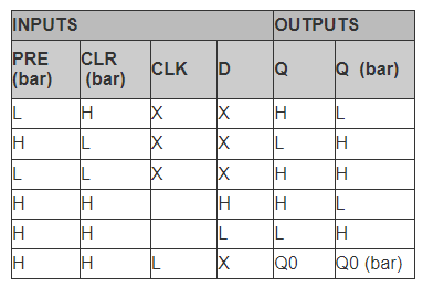
When PRE and CLR are high, the D flip-flop operates normally. On the rising edge of the clock signal, the value of Q will be set to the value of D. When PRE is low, Q is directly set to high level, and when CLR is low level, Q is set to low level.
74LS74 Application:
State storage: D flip-flops can be used as state storage to store bit data.
Data transfer: Data can be transferred under specific clock pulses.
Edge detection: can be used to detect rising or falling edges of clocks or other signals.
Frequency divider: By feeding the Q output back to the D input, a frequency divider of 2 can be achieved.
Double D flip-flops can be used independently or in series: in some applications, two flip-flops may be required to perform a specific sequence of operations.
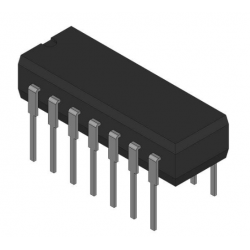
74LS74 pin assignment


74LS74 Features
Double D flip-flop package IC
Operating voltage: 2V to 15V
Propagation delay: 40nS
Minimum high level input voltage: 2V
Maximum low-level input voltage: 0.8V
Operating temperature: 0 to 70°C
High level output current: 8mA
Available in 14-pin SO-14, SOT42 packages
74LS74 Equivalent/Replaceable Products
74LVC2G80 ,HEF40312B ,74LS74APC ,74LS74APCQR ,74LS74ASC ,74LS74PC ,SN74LS74A , SN74LS74ADBR ,SN74LS74AN , SN74LS74ANSRG4 ..,the models are sold on the jinftry official website, they are all original and authentic, with obvious price advantages. Welcome to consult via email or Skype
What is 74LS74?
The 74LS74 IC is a dual D-type edge-triggered flip-flop equipped with clear preset functions and complementary output terminals. The IC can retain data in binary form with the flexibility to modify the stored data if necessary. It demonstrates a high operating voltage range for various functional prerequisites and facilitates seamless connectivity with CMOS, TTL and NMOS systems. When a low level appears on the preset input, the output is adjusted based on the logic level of the given input. The D-type flip-flop is also called a data flip-flop or a delayed flip-flop. It is designed to capture the D input value at a specific point within a signal or clock cycle, such as the falling edge of a clock signal. Data at the D input passes through the flip-flop on the positive edge of the pulse.
How to use 74LS74
Use Vcc and GND pins to power the IC. As mentioned before, each trigger operates independently. Connect the input signal to pins 2 and 3 to enable the first flip-flop and the output is reflected on pins 5 and 6. Pin 3 requires a clock source, usually a PWM signal from an MCU or a 555 timer. Activating the pin to the high state will clear the data and reset the flip-flop. To clearly understand its operation, please refer to the function table provided below. In this table, the "X" means "uncorrelated" and the upward arrow represents the rising edge of the signal.

How to use 74LS74
74LS74 Manufacturer:
Fairchild Semiconductor
National Semiconductor
ON Semiconductor
74ls74 datasheet:

edit author:
![]()
Jinftry(Hong Kong registered company name: JING FU CAI (HONGKONG) INTERNATIONAL CO., LIMITED) was established in 2013, headquartered in Hong Kong, China, with a branch in Shenzhen, China. It is a global supplier of electronic components and a well-known and competitive electronic product distributor in Asia. Is also an excellent strategic partner of global ODM/OEM/EMS, able to quickly find authentic and traceable electronic components for customers to purchase.


