A comprehensive introduction to the basic knowledge of PCBA
Comprehensive introduction and development trend of PCBA basic knowledge
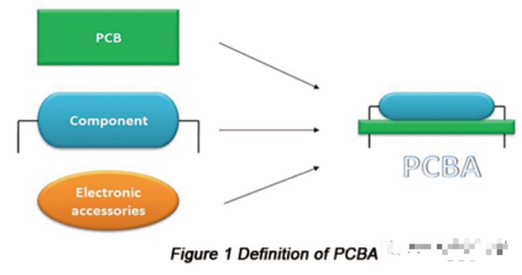
PCBA (Printed Circuit Board Assembly) refers to a printed circuit board that has been pasted with electronic components, which is what we often call circuit board assembly or printed circuit board assembly. It is to make the bare printed circuit board (PCB) into a complete circuit system or module of electronic products through SMT surface mount, DIP plug-in and other processes.
It mainly includes the following steps:
SMT (Surface Mount Technology): Surface mount technology, by mounting electronic components on the surface of the PCB.
DIP (Dual In-line Package): plug-in technology, for those components that are not suitable for surface mount, such as large, high heat or specific function components.
Soldering: Ensuring a solid and electrical connection between components and the board.
Testing: usually includes ICT (In-Circuit Test) and functional testing to ensure that the PCBA is functioning properly.
Assembly type of PCBA
The main assembly types of PCBA are shown in Table 1 below.
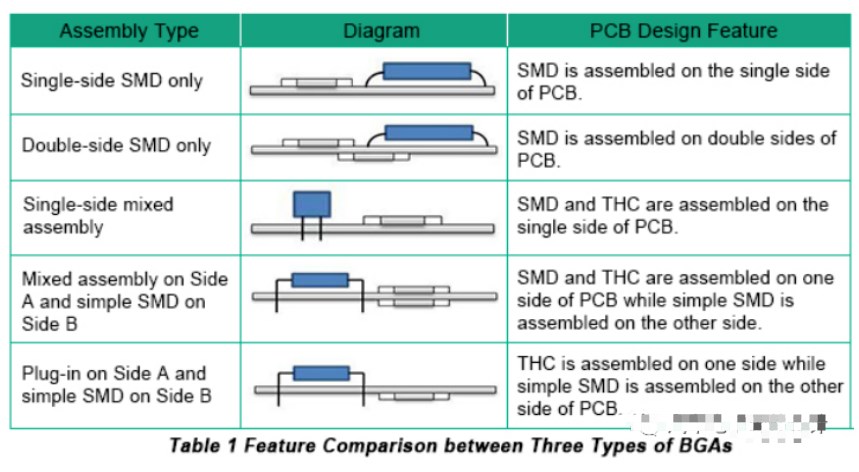
So far, single-sided SMD and double-sided SMD are mainly used in power boards and communication backplanes, while other assembly types are used in complex devices such as computers, DVDs, and mobile phones.
SMT program
The SMT process belongs to a soldering process that melts the solder paste pre-distributed on the PCB pad through a reflow oven to achieve mechanical and electrical connections between the SMD solder joints or pins and the PCB pad. Suitable for all kinds of SMD soldering. The main steps of SMT include solder paste printing, component mounting and reflow soldering.
• Solder paste printing station
This site is mainly composed of solder paste, models and solder paste printers. The solder paste is first printed on the corresponding position of the PCB from a professional solder paste model by a solder paste printer. Electronic component soldering is then completed by component mounting and reflow soldering.
• Component mounting table
The station is mainly composed of SMD, loader and placement machine. The SMD is mounted on a specific position of the PCB by a component loader and a professional placement software program, and is soldered by reflow. The placement machine is divided into a high-speed placement machine and a general-purpose placement machine. The former is suitable for the mounting of crystal chips and small components, and the latter is suitable for the mounting of ICs, irregular and large components.
• Reflow soldering station
The station mainly consists of a reflow oven. SMD welding is to make the PCB with mounted components pass through the reflow oven, set the welding parameters, and realize component welding. The reflow oven mainly includes infrared heating and hot air heating.
• Wave soldering process
In the wave soldering process, the molten solder is converted into the required solder wave by mechanical bumps or electromagnetic bumps with jet characteristics. The PCB on which the components are assembled must then pass through a solder wave for mechanical and electrical soldering between component solder points or PCB pads.
The key steps of wave soldering include component forming, component insertion or mounting, soldering and cooling by solder wave. This means inserting molded components onto the PCB as needed. Then the PCB loaded with components is pushed into the wave soldering system through the transmission device. Next the flux is sprayed and the PCB will be preheated in the preheat zone. The final step is wave soldering and cooling.
• Component molding and plug-in components
The main work of this station is to preform some components to meet the requirements of mounting, plugging and wave soldering.
• Wave soldering
The main work of wave soldering is to plug the molded components where they are needed according to certain requirements. Then the PCB filled with components enters the wave soldering system through the transmission device. First, the flux is sprayed, and the PCB is preheated in the preheating zone. Next comes wave soldering and the final step is cooling.
Welding Basics
Welding can be divided into the following three categories: fusion welding, bonding and brazing, as shown in Figure 3.

In addition, there are other categories of welding such as ultrasonic bonding, gold ball bonding, and laser welding.
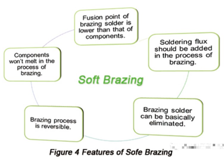
Brazing can be divided into hard brazing and soft brazing. The former refers to high-temperature, large-scale welding, and the latter refers to relatively low-temperature, small-scale welding, such as component welding. Regarding some aspects of soldering, the following content is added.
a Definition: Soldering refers to brazing at a temperature lower than 450°C.
b Features: The figure below shows the characteristics of soldering.
cBasic theory
When the metal is welded, the metal to be welded is heated to a certain temperature range, the oxide layer and pollutants are removed under the activation of the flux, and the metal surface will obtain sufficient activation energy. Molten solder melts, wets, expands and joins metallurgically. Due to the fusion between the solder and the metal surface to be welded, the solder will solidify after cooling to form a solder joint. The tensile strength is related to the lattice structure between the metals and the thickness of the bonding layer.
d. Brazing process: The main process of soldering includes wetting, diffusion, dissolution and metallurgical bonding.
The development trend of PCBA:
Miniaturization and high integration: With the advancement of technology, components are getting smaller and smaller, but their functions are getting more powerful. This leads to more and more complex PCBA design and higher integration.
Intelligent manufacturing and automation: In order to improve production efficiency and quality, more automation and intelligent manufacturing technologies have been introduced into the PCBA production line, such as automatic robot loading, AI-driven inspection technology, etc.
Environmental protection and sustainability: Due to the demand for environmental protection, low-toxic or non-toxic solder, recyclable materials, and energy-saving designs are getting more and more attention.
Flexible and wearable technology: With the development of wearable devices and flexible electronics, flexible PCBA has gradually become a new development direction, providing support for new products such as folding screen mobile phones, flexible screens, and smart clothing.
High frequency and high speed: With the development of 5G, 6G and ultra-high-speed computing, PCBA design will need to meet higher frequency and speed requirements.
Modularization and standardization: In order to shorten the time to market and reduce costs, modular and standardized design methods will also become more and more popular.
Multi-technology integration: With the development of technologies such as IoT, AI, and edge computing, PCBA will not only be a pure hardware platform, but also need to integrate multiple technologies to meet diverse application requirements.
In general, the development of PCBA will place more emphasis on technological innovation, ecological environment protection and the challenges of meeting diversified needs, providing a solid support for the further development of the electronics industry.

The difference between PCB and PCBA
PCB is the abbreviation of printed circuit board. It is an important electronic component loaded with electronic components and a connection carrier for the conduction of electronic components. It is so called because of a printing technique used.
PCB is divided into single-layer, double-sided and multi-layer according to the circuit layer. Typical are 4-layer and 6-layer multilayer PCBs. More complex multilayer PCBs have dozens of layers. It can also be divided into rigid board, flexible board and flexible rigid board. Printed boards have developed from single-layer to double-sided, multi-layer, and flexible boards, maintaining their respective development trends.
PCB
PCBA: Printed Circuit Board Assembly, circuit board assembly is a term in the electronic processing industry, mainly refers to the welding or insertion of various electronic parts, IC and other materials on a blank circuit board and quality inspection and testing to ensure that it has a complete circuit connection performance.
The blank board is made according to the customer's PCB file. Therefore, there are no electronic components on the whiteboard, just various pads. Installing electronic components on the PCB, installing electronic components is SMT processing, that is, soldering electronic parts on the pad, and then need to use DIP plug-in to assist processing to complete the entire welding process.
edit author:
![]()
Jinftry(Hong Kong registered company name: JING FU CAI (HONGKONG) INTERNATIONAL CO., LIMITED) was established in 2013, headquartered in Hong Kong, China, with a branch in Shenzhen, China. It is a global supplier of electronic components and a well-known and competitive electronic product distributor in Asia. Is also an excellent strategic partner of global ODM/OEM/EMS, able to quickly find authentic and traceable electronic components for customers to purchase.


