TI TPS6287x-Q1 Synchronous Buck Converters
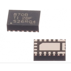
TI TPS6287x-Q1 Synchronous Buck Converters
TI TPS6287x-Q1 Synchronous Buck Converters are a family of pin-to-pin 6A, 9A, 12A, and 15A step-down DC/DC converters with differential remote sensing. Each current rating is available as a full-featured part version with an I2C interface and a limited-function part version that does not require an I2C interface. All devices are highly efficient. The low-resistance power switch supports up to 15A of continuous output current at high ambient temperatures. Each device can operate in stack mode for higher output current. The device can also be used to increase power dissipation on multiple devices.
TI's TPS6287x-Q1 family uses an enhanced DCS control scheme to support fast transients for fixed frequency operation. The devices operate in power-save mode for maximum efficiency or in forced-PWM mode for excellent transient performance with the lowest output voltage ripple. An optional remote sense feature maximizes voltage regulation at the point of load. The device achieves better than ±1% dc voltage accuracy under all conditions. The switching frequency is resistor selectable with the FSEL pin. The switching frequency can be programmed to 1.5MHz, 2.25MHz, 2.5MHz, or 3.0MHz, or synchronized to an external clock within the same frequency range.
The I2C-compatible interface has a variety of control, warning, and monitoring features. These include voltage monitoring and temperature-related warnings. The output voltage can be adjusted through an I2C-compatible interface to quickly adjust the power consumption of the load according to the performance needs of the application. The default start-up voltage is resistor selectable through the VSEL pin.
characteristic
AEC-Q100 Qualified for Automotive Applications
Temperature class 1 TA: –40°C to +125°C
Supports functional safety
Documentation to aid functional safety system design
Input voltage range: 2.7V-6V
6A, 9A, 12A, and 15A Series Pin-to-Pin Compatible Devices
Four output voltage ranges
0.4V-0.71875V (1.25mV step)
0.4V-1.0375V (2.5mV step)
0.4V-1.675V (5mV step)
0.8V-3.35V (10mV step)
Output voltage accuracy: ±1%
7mΩ and 4.5mΩ Internal Power MOSFETs
Adjustable external compensation
Resistor Selectable Startup Output Voltage
Resistor Selectable Switching Frequency
Power Saving and Forced PWM Operation
I2C compatible (up to 1MHz)
Differential Remote Sensing
Optional stacking operation for increased output current capability
Thermal Warning and Thermal Shutdown
Precision Enable Input
Active output discharge
Optional Spread Spectrum Clocking
Power Good Output with Window Comparator
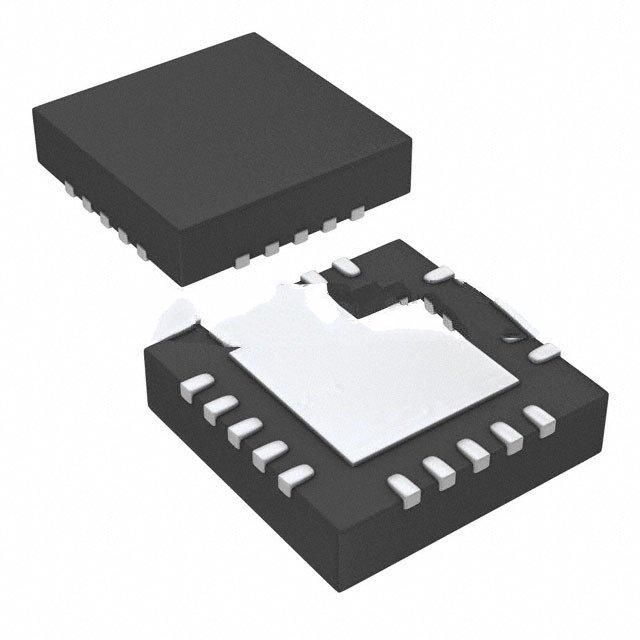
Packaged in 2.55mm × 3.55mm × 1mm VQFN

