Texas Instruments TCAN1463-Q1 High-Speed CAN FD Transceiver
Texas Instruments TCAN1463-Q1 High-Speed CAN FD Transceiver
Texas Instruments TCAN1463-Q1 High-Speed CAN FD Transceiver
The TCAN1463-Q1 high-speed controller area network FD transceiver complies with the physical layer requirements of the ISO 11898-2:2016 high-speed CAN specification and the CiA 601-4 SIC specification. The device supports legacy CAN and CAN FD with data rates up to 8MB/s. The TCAN1463-Q1 reduces signal ringing at the dominant-to-recessive edge and enables higher throughput in complex network topologies. The SIC enables applications to operate at 2Mbps, 5Mbps or higher in large networks with multiple unterminated studs, thereby exploiting the real benefits of CAN FD. The device is pin compatible with legacy CAN FD transceivers such as the TCAN1043A-Q and TCAN1043-Q1.
Texas Instruments TCAN1463-Q1 reduces battery current consumption by selectively enabling various power supplies that may be present on the system through the INH output pin. This feature enables a low current sleep state where power is passed to all system components except the TCAN1463-Q1 while monitoring the CAN bus. When a wake-up event is detected, the TCAN1463-Q1 starts the system by driving INH high. The TCAN1463-Q1 features a SWE timer that safely transitions to sleep mode after 4 minutes of inactivity in standby mode. This feature ensures that the device transitions to a low-power sleep mode if the MCU fails to transition the device to normal mode.
characteristic
AEC-Q100 qualified for automotive applications (Tier 1)
Support for functional safety
Documentation available to assist in the design of functional safety systems
Meet the requirements of ISO 11898-2:2016
Implements the Signal Improvement Function (SIC) as defined in CiA 601-4
Actively improve bus signals by eliminating ringing and enhancing bit symmetry
Supports legacy CAN and CAN FD up to 8Mbps
Wide input operating voltage range
VIO level shifting support (1.7V-5.5V range)
low power sleep mode
High voltage INH output for system power control
INH_MASK pin to keep INH disabled during spurious wake-up events
Local wake-up support via WAKE pin
Sleep Wake Error (SWE) timer enables safe transition from standby to sleep in the event of a system power failure or software failure
Longer power-up time possible
Define behavior when not powered
Bus and IO terminals are high impedance (no load on running bus or application)
Protection features
±58V CAN bus fault tolerance
VSUP load dump support
IEC ESD protection
Undervoltage protection
Thermal Shutdown Protection
TXD Dominant State Timeout (TXD DTO)
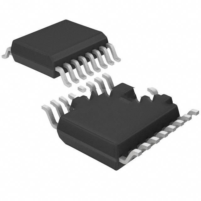
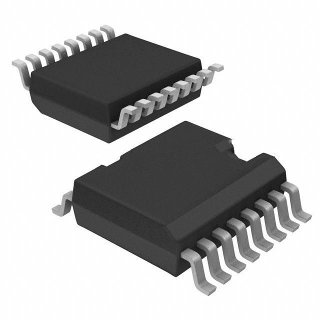
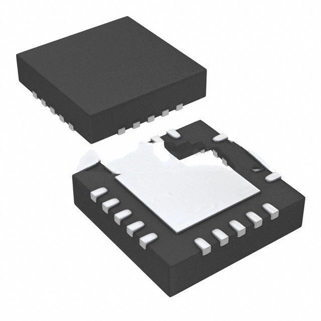
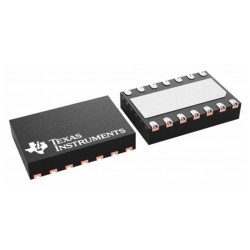
Available in 14-pin leaded (SOT and SOIC) and leadless (VSON) packages with wettable flanks for enhanced automatic optical inspection (AOI) capabilities
application
Body Electronics and Lighting
Automotive Gateway
Advanced Driver Assistance Systems (ADAS)
Infotainment & Dashboard
Hybrid, Electric and Powertrain Systems
Personal Transportation - Electric Bikes

