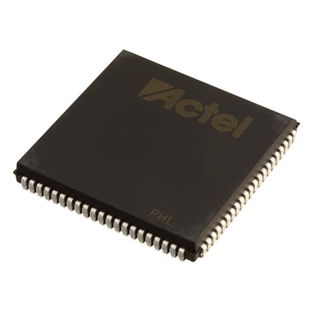
A42MX16-3PLG84 vs MPF200T-FCG784E
| Part Number |

|

|
| Category | Embedded - FPGAs (Field Programmable Gate Array) | Embedded - FPGAs (Field Programmable Gate Array) |
| Manufacturer | Microchip Technology | Microchip Technology |
| Description | IC FPGA 72 I/O 84PLCC | IC FPGA 364 I/O 784FCBGA |
| Package | Tray | Tray |
| Series | MX | PolarFire™ |
| Voltage - Supply | 3V ~ 3.6V, 4.75V ~ 5.25V | 0.97V ~ 1.08V |
| Operating Temperature | 0°C ~ 70°C (TA) | 0°C ~ 100°C (TJ) |
| Mounting Type | Surface Mount | Surface Mount |
| Package / Case | 84-LCC (J-Lead) | 784-BBGA, FCBGA |
| Supplier Device Package | 84-PLCC (29.31x29.31) | 784-FCBGA (29x29) |
| Number of I/O | 72 | 364 |
| Number of Gates | 24000 | - |
| Number of LABs/CLBs | - | - |
| Number of Logic Elements/Cells | - | 192000 |
| Total RAM Bits | - | 13619200 |
-
1. What is the hardware of FPGA?
FPGA (Field Programmable Gate Array) is a highly flexible programmable logic chip that users can program to achieve specific logic functions according to their needs. The main uses of FPGA include communications and networks, digital signal processing, automotive and aerospace, industrial automation, high-performance computing, smart Internet of Things and many other aspects.
-
2. Is FPGA a microcontroller?
FPGA is not a microcontroller. There are significant differences between FPGA and microcontroller in terms of function and use.
FPGA is a programmable integrated circuit, which is programmed through hardware description language and can customize the circuit according to needs. It is very suitable for application scenarios that require flexible configuration and high performance. In contrast, microcontrollers (MCUs) are integrated circuits with preset functions, usually used for single tasks and requiring efficient execution.
FPGAs and MCUs also differ in structure and application scenarios. FPGAs offer great flexibility and are suitable for complex applications that require rapid prototyping and reconfigurability. On the other hand, MCUs combine processor cores, memory, and various peripherals in a single chip, designed for specific tasks, and provide cost-effective solutions. -
3. Is FPGA faster than CPU?
FPGAs are faster than CPUs in some cases. FPGAs are programmable hardware devices whose internal architecture can be configured by users as needed, which enables them to process multiple computing tasks in parallel, resulting in higher computing performance in some scenarios.
FPGAs and CPUs have different architectures and design goals. CPUs are general-purpose processors that can perform a variety of tasks, but may require multiple clock cycles to process specific operations. FPGAs, on the other hand, achieve specific computing structures by reorganizing circuits, and have higher parallelism and efficiency. For example, when processing specific tasks such as signals and images, FPGAs can complete them faster than CPUs.
The main advantage of FPGAs is their programmability and flexibility. FPGAs can be reprogrammed and reconfigured as needed, which enables designers to quickly test new and updated algorithms without developing and releasing new hardware, thereby speeding up time to market and saving costs. In addition, FPGAs offer the advantages of superior performance and reduced latency, and are suitable for real-time applications that require low latency and deterministic latency. -
4. Is FPGA analog or digital?
FPGAs are digital. FPGAs (field programmable gate arrays) are integrated chips that are mainly digital circuits, not analog. FPGAs are a type of programmable logic device that processes digital signals instead of analog signals.
FPGAs are a type of programmable logic device, a type of programmable logic device (PLD). It solves the shortcomings of traditional custom circuits, while also overcoming the shortcomings of the limited number of gate circuits in the original programmable devices. FPGA is a product that is further developed on the basis of traditional logic circuits and gate arrays such as PAL (Programmable Logic Array), GAL (General Array Logic), and CPLD (Complex Programmable Logic Device).
The design process of FPGA includes the use of computer-aided design, by drawing schematic diagrams that implement user requirements, editing Boolean equations, or using hardware description languages as design inputs. Then after a series of conversion programs, automatic layout and routing, and simulation processes, the FPGA data file is finally generated to initialize the FPGA device.

