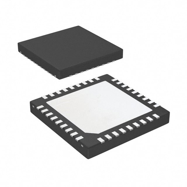
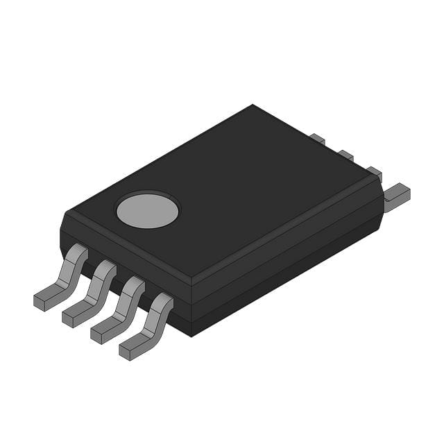
LMK00306SQ/NOPB vs CDCV304TPWREP
| Part Number |

|

|
| Category | Clock/Timing - Clock Buffers, Drivers | Clock/Timing - Clock Buffers, Drivers |
| Manufacturer | Texas Instruments | Texas Instruments |
| Description | IC CLK BUFFER 3:7 3.1GHZ 36WQFN | IC CLK BUFFER 1:4 200MHZ 8TSSOP |
| Package | Tape & Reel (TR) | -Reel® |
| Series | - | - |
| Type | Fanout Buffer (Distribution), Multiplexer, Translator | Fanout Buffer (Distribution) |
| Voltage - Supply | 3.15V ~ 3.45V | 2.3V ~ 3.6V |
| Operating Temperature | -40°C ~ 85°C | -40°C ~ 105°C |
| Mounting Type | Surface Mount | Surface Mount |
| Package / Case | 36-WFQFN Exposed Pad | 8-TSSOP (0.173\", 4.40mm Width) |
| Supplier Device Package | 36-WQFN (6x6) | 8-TSSOP |
| Output | HCSL, LVCMOS, LVDS, LVPECL | LVTTL |
| Frequency - Max | 3.1 GHz | 200 MHz |
| Number of Circuits | 1 | 1 |
| Input | CML, HCSL, HSTL, LVDS, LVPECL, SSTL, Crystal | LVTTL |
| Ratio - Input:Output | 3:7 | 1:4 |
| Differential - Input:Output | Yes/Yes | No/No |
-
1. What is the difference between a clock buffer and a clock driver?
The main function of a clock buffer is to distribute clock signals, while a clock driver is used to enhance signal strength to drive higher loads. Buffer is usually used for branching and synchronizing multiple clock signals, while driver is used to increase signal transmission distance and load capacity.
-
2. What is the function of a clock driver?
The function of a clock driver is to enhance the driving capability of the clock signal, ensuring that the signal can be transmitted further or drive more loads without causing signal attenuation or distortion. It is particularly important in high-frequency and high load applications.
-
3. What output configurations does the clock buffer support?
Clock buffers typically support multiple output configurations, including single ended output, differential output, programmable delay, or selectable output frequency, to accommodate different system requirements.
-
4. How to evaluate the performance of clock drivers?
When evaluating clock drivers, several key parameters need to be considered:
Driving capability (load capacity)
Output signal integrity
Phase noise and jitter
Power noise suppression
Power supply voltage range and power consumption

