NXP USA Inc. PBSS4140DPN/DG/B2115

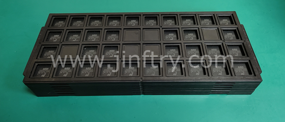
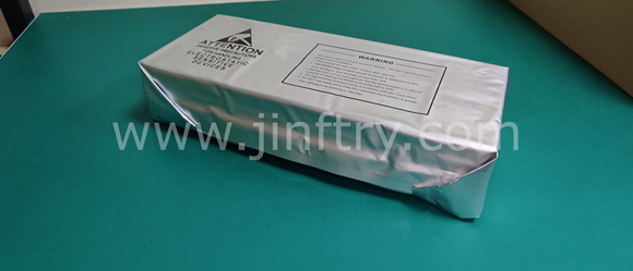
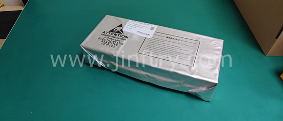
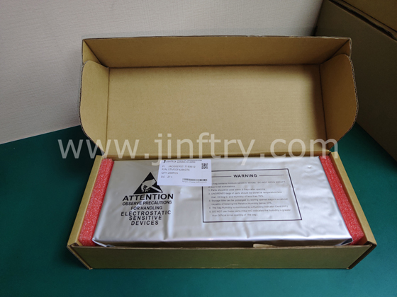
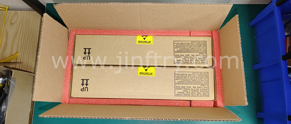
The picture is for reference only, please refer to the product specification
- PBSS4140DPN/DG/B2115
- NXP USA Inc.
- SMALL SIGNAL BIPOLAR TRANSISTOR
- Transistors - Bipolar (BJT) - Single
- PBSS4140DPN/DG/B2115 Datasheet
- -
- Bulk
-
 Lead free / RoHS Compliant
 - 1569
- Spot Inventory / Athorized Dstributor / Factory Excess Stock
- 1 year quality assurance 》
- Click to get rates


What is PBSS4140DPN/DG/B2115
NXP USA Inc. Part Number PBSS4140DPN/DG/B2115(Transistors - Bipolar (BJT) - Single), developed and manufactured by NXP USA Inc., distributed globally by Jinftry. We distribute various electronic components from world-renowned brands and provide one-stop services, making us a trusted global electronic component distributor.
PBSS4140DPN/DG/B2115 is one of the part numbers distributed by Jinftry, and you can learn about its specifications/configurations, package/case, Datasheet, and other information here. Electronic components are affected by supply and demand, and prices fluctuate frequently. If you have a demand, please do not hesitate to send us an RFQ or email us immediately [email protected] Please inquire about the real-time unit price, Data Code, Lead time, payment terms, and any other information you would like to know. We will do our best to provide you with a quotation and reply as soon as possible.
PBSS4140DPN/DG/B2115 Specifications
- Part NumberPBSS4140DPN/DG/B2115
- CategoryTransistors - Bipolar (BJT) - Single
- ManufacturerNXP USA Inc.
- DescriptionSMALL SIGNAL BIPOLAR TRANSISTOR
- PackageBulk
- Series-
- Operating Temperature-
- Mounting Type-
- Package / Case-
- Supplier Device Package-
- Power - Max-
- Transistor Type-
- Current - Collector (Ic) (Max)-
- Voltage - Collector Emitter Breakdown (Max)-
- Vce Saturation (Max) @ Ib, Ic-
- Current - Collector Cutoff (Max)-
- DC Current Gain (hFE) (Min) @ Ic, Vce-
- Frequency - Transition-
Application of PBSS4140DPN/DG/B2115
PBSS4140DPN/DG/B2115 Datasheet
PBSS4140DPN/DG/B2115 Datasheet , Bulk
PBSS4140DPN/DG/B2115 Classification
Transistors - Bipolar (BJT) - Single
FAQ about Transistors - Bipolar (BJT) - Single
-
1. Is BJT bipolar or unipolar?
BJT (bipolar junction transistor) is bipolar. BJT (bipolar junction transistor) is composed of two N-type semiconductors sandwiched between a P-type semiconductor, with an emitter junction formed between the emitter and the base, and a collector junction formed between the collector and the base. When the power is turned on, the majority carriers (electrons) in the emitter and the majority carriers (holes) in the base diffuse with each other, forming a current amplification effect.
The working principle of BJT is to achieve current amplification through the control of two PN junctions (emitter junction and collector junction). When the emitter junction is forward biased, electrons are injected from the emitter region into the base region; when the collector junction is reverse biased, electrons are injected from the base region into the collector region. Because the base region is very thin and the impurity content is strictly controlled, most electrons can enter the collector region through the collector junction to form the collector current Ic, and only a small number of electrons recombine with holes in the base region to form the base current Ib. Therefore, by controlling the base current Ib, the collector current Ic can be amplified to achieve current amplification. -
2. What is the difference between bipolar transistors and CMOS transistors?
The main differences between bipolar transistors and CMOS transistors are in working principles, structures, application scenarios, and power consumption.
Working principle
Bipolar transistor: Bipolar transistors have two types of carriers (holes and electrons) involved in conduction, and they are made of three parts of semiconductors with different doping levels. In bipolar transistors, the emitter emits free electrons, the collector receives holes, and the base controls the on and off of the current.
CMOS transistor: CMOS transistors have only one type of carrier (electrons or holes) involved in conduction, usually using a combination of P-type semiconductors and N-type semiconductors. In CMOS transistors, when the gate voltage is zero, the current does not flow. Only when the gate voltage reaches a certain value, the current will flow, which makes the CMOS transistor consume almost no power when static.
-
3. What are the two types of BJT transistors?
There are two main types of BJT transistors: NPN and PNP.
NPN transistor
In an NPN transistor, current flows from the collector to the emitter. The base of an NPN transistor must be connected to a positive voltage for current to flow in. As the current flowing to the base increases, the transistor gradually turns on until the current is completely conducted from the collector to the emitter.
PNP Transistor
In a PNP transistor, the current flows from the emitter to the collector. Therefore, the base of the PNP transistor must be grounded. When the output current is small and the base is negative relative to the emitter, the transistor will turn on and a larger current will flow from the emitter to the collector. Basically, if the base and collector are negative relative to the emitter, the PNP transistor will conduct current from the emitter to the collector.
We are a professional PCB manufacturer who offers comprehensive PCB manufacturing services including: professional Ceramic PCB HDI PCB Heavy Copper PCB High-TG PCB High Speed PCB High Frequency PCB Metal Core PCB PCB fabrication and PCB assembly, providing fast turnaround prototypes for high-end products.


• Prompt Responsiveness
• Guaranteed Quality
• Global Access
• Competitive Market Price
• One-Stop support services of supply chain
Jinftry, Your most trustworthy component supplier, welcome to send us the inquiry, thank you!
Do you have any questions about PBSS4140DPN/DG/B2115 ?
Feel free to contact us: