Development status and future prospects of high-temperature SOI technology
Development status and future prospects of high-temperature SOI technology
Silicon-on-insulator (SOI) is a semiconductor wafer technology that produces devices with higher performance and lower power consumption (dynamic) than traditional bulk silicon technology. SOI works by placing a thin insulating layer, such as silicon oxide, between a thin layer of silicon and a silicon substrate. This process helps reduce junction capacitance, thereby increasing speed and reducing power consumption. SOI chips can be 15 percent faster and consume 20 percent less power than today's chips based on bulk complementary metal-oxide semiconductors (CMOS).

Figure 1 Cross-sectional view of an SOI structure

Figure 2 Cross-sectional view of p-n junction isolation
The demand for commercial applications of high-temperature electronics originally came from the fields of oil and natural gas exploration and production. The ambient temperature of drilling continues to increase with the increase of well depth. When the well depth exceeds 7000 m, the downhole temperature can exceed 200°C. In the aerospace field, the electronic devices of the spacecraft may be exposed to high temperature environments due to their own heating and external factors. The high cost and high risk of aerospace projects make them particularly pursue high-temperature, high-reliability electronic devices. Aviation applications require high safety, reliability and maintainability. High-temperature resistant electronic devices make distributed control of aircraft engines and other components possible, and also make it possible to eliminate or weaken the original complex and bulky liquid cooling and hydraulic transmission. system possible. In recent years, third-generation wide-bandgap semiconductors (WBG) such as SiC, which have inherent high-temperature resistance, have become increasingly mature and fully commercialized. They form an ideal match with high-temperature-resistant silicon-on-insulator (SOI) devices, which not only promotes It has promoted the development of high-temperature applications in traditional fields such as petroleum and aerospace, and has also driven new high-temperature applications in various industrial fields such as high-speed rail, electric vehicles, and mobile energy storage.
High-temperature SOI technology breaks through the high-temperature dilemma of bulk silicon semiconductor devices. It is very complementary to SiC power devices in terms of circuit types. It can help the development of high-temperature electronic technology reach a new level and has broad application prospects. This article provides a detailed introduction to the development status of high-temperature SOI technology, and conducts an in-depth discussion of its future development direction and application prospects.
High temperatures can cause performance degradation in ordinary bulk silicon semiconductor devices. When the temperature rises to 150 to 200°C, the intrinsic carrier concentration of the silicon base increases significantly. Not only is the silicon base substrate almost completely conductive, but the PN junction barrier has been thinned to almost disappear, resulting in the basic functions of the semiconductor. Collapse, the semiconductor at this time has almost become a conductor.
Semiconductor devices work through PN junctions formed by doping. Their basic electrical properties rely on carriers. Doping carriers play a decisive role. Temperature is the main auxiliary factor in the work of doped carriers. Under certain temperature conditions, sufficient thermal motion enables the doping atoms to be fully ionized, and the majority carriers (majority carriers) carried by the doping atoms can fully function and cooperate with the minority carriers (minority carriers). The basic properties of semiconductors are constructed. Appropriate temperature is an important auxiliary factor for the semiconductor to enter normal operation. Excessive temperature will damage the performance of the semiconductor. As the temperature increases, the intrinsic carrier concentration will also accelerate and the PN junction barrier will be reduced. Thin, the key indicators of semiconductors gradually decrease. When the temperature reaches a certain threshold, the concentration of intrinsic carriers will drown out the concentration of carriers contributed by doping materials, causing the semiconductor performance to be extremely weakened or even disappear, which will lead to The collapse of fundamental characteristics of semiconductors.
Doping concentration is the first key factor in semiconductor performance. The higher the doping concentration, the higher the saturation ionization temperature range in which the semiconductor works normally. The doping concentration of conductor materials is limited by the solubility characteristics of the material itself, and its maximum doping concentration has a certain limit. Theoretical and experimental research results have proven [1-4] that for bulk silicon semiconductor devices, the increase in temperature leads to changes in the physical properties of the material, the bandgap width decreases, and the intrinsic carrier concentration increases, between 125 and 150 °C range, the intrinsic carrier concentration begins to catch up with the doping carrier concentration. Compared with bulk silicon semiconductors, semiconductor materials with larger bandgaps have lower intrinsic carrier concentrations at the same temperature, and the temperature threshold beyond doping carrier concentration is higher, so they have higher normal operation. Temperature zone. Generally speaking, the maximum normal operating temperature boundary of germanium devices is 100°C, silicon is 250°C, gallium arsenide is 450°C, and SiC exceeds 600°C.
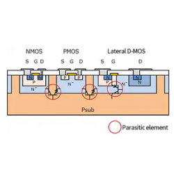
When the junction temperature exceeds 125°C, the performance of the bulk silicon semiconductor rapidly weakens, or even fails to work properly at all. The biggest cause is the rapid increase in leakage current. Research results show [4-6] that the leakage current of bulk silicon metal oxide semiconductor field effect transistor (MOSFET) is not only strongly related to the intrinsic carrier concentration, but also proportional to the junction area and depletion region width. Therefore, many researchers hope to reduce the PN junction area and depletion region width by improving the device structure, thereby reducing leakage current and improving the high-temperature performance of the device. High-temperature SOI technology emerged as the times require. High-temperature SOI technology not only improves the high-temperature performance of the device, but also improves the overall electrical performance of the device;
What is more realistic is that, except for some special process links that require special equipment, a large part of the SOI process can use the manufacturing equipment and processes of traditional bulk silicon devices, showing great commercial feasibility.


