What is a gallium nitride(GaN) transistor? The difference between GaN and silicon
What is a gallium nitride(GaN) transistor? The difference between GaN and silicon
Gallium nitride (GaN) is a semiconductor material known for its excellent electronic properties, especially for applications in high-frequency and high-power devices. Gallium nitride has a large band gap width, high thermal conductivity and electron mobility, which makes it perform well under extreme conditions, such as high temperature and high voltage environments.
Gallium nitride (GaN) transistors are high electron mobility (HEMT) semiconductor devices consisting of three terminals: gate, source, and drain. High electron mobility means GaN transistors have higher electric field strengths compared to silicon-based transistors. GaN transistors have the advantages of low on-state resistance, low conduction loss, low switching loss, high-frequency switching, high efficiency, small size, high power density, and high temperature resistance.
GaN transistors are ideal for consumer power supplies, multi-level converters, solar inverters, industrial motor drives, UPS, high voltage battery chargers, telecom, SMPS, totem pole PFC, high frequency LLC, and enterprise and network power applications.
GaN is a compound formed from gallium (atomic number 31) and nitrogen (atomic number 7). Gallium does not exist in elemental form, so it is a by-product when bauxite ore is smelted into aluminum and sphalerite ore is processed into zinc.
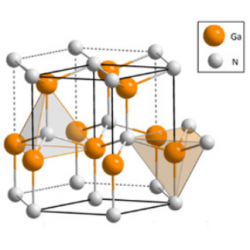
The atomic structure of GaN wurtzite crystal is as follows:

The resulting hexagonal crystal structure is very strong and stable, with a melting point of 4532°F/1700°C. This means GaN can operate at higher temperatures than its silicon counterparts. It also has a larger band gap compared to silicon. The band gap is the energy required to detach an electron from its orbit. At room temperature, GaN is insoluble in water, acids and alkalis. GaN also has a high electron mobility of 2000 cm 2 /Vs, which makes it suitable for high frequency applications (in the 1 THz range).
Figure of Merit is a relative measure of the inherent, frequency-independent power handling capability of the base material. GaN has a slightly lower thermal conductivity than silicon, but because it is more efficient, it operates cooler than silicon-based devices at high voltages.
The following table summarizes the differences between GaN and silicon:
| Parameters | GaN | Silicon |
| Wafer Diameter | 3-6 inches | 8 inches |
| Maximum Frequency | 1 THz | 3.8 GHz |
| Maximum Temperature | 600 ̊C | 150 ̊C |
| Peak Electron Velocity | 2.7 x 10⁵m/s | 1 x 10⁵ m/s |
| Band Gap | 1.1 eV | 3.4 eV |
| Electric Field | 3.3 MV/cm | 0.3 MV/cm |
| Power Density | 0.8 W/mm | 7W/mm |
| Thermal Conductivity | 1.3 W/cmK | 1.5 W/cmK |
| Figure of Merit | 3000 mn*Ec 3 | 1 mn*Ec 3 |
| Johnson Figure of Merit | 27.5 [Ec*vsat]/2p | 1 [Ec*vsat]/2p |
Compared with other semiconductor technologies, GaN devices have significant advantages in reducing energy costs because GaN is more efficient than silicon and therefore dissipates less energy in the form of heat, thus reducing cooling costs and reducing the need for cooling systems (e.g. radiator, fan, etc.).
GaN also offers higher power density, which reduces system size and associated magnetic and parasitic issues. It provides higher switching frequency, which means less switching losses and fewer inductive and capacitive components required in the power circuit. This results in systems that are smaller in size and weight, generate less interference and noise, require less filtering, and provide greater spatial freedom during the design process.
While GaN devices have many clear advantages over silicon devices, there are also some disadvantages. Gallium nitride semiconductors are more expensive to manufacture than silicon semiconductors. However, the high cost of GaN is compensated by significantly lower auxiliary and overall system costs. Overall savings are typically 10-20%. Due to its complex manufacturing and manufacturing processes, the dislocation density is quite high (108~1010/cm2), although efforts are being made to reduce the dislocation density. Crystallizing GaN from molten material is not possible because the process of developing bulk GaN crystals is more challenging compared to Si. Commercialization of bulk gallium nitride is difficult to achieve not only because of the high cost and small size of these substrates, but also because of the huge initial investment required to establish a dedicated gallium nitride fab, which drives up the average selling price of the device, further hindering mass production. These devices are adopted by the industry.
Another major disadvantage is the difficulty in forming ohmic contacts. GaN is a wide-bandgap semiconductor with excessive polarity, making it difficult to obtain good metal-semiconductor ohmic contact through high doping, which is a problem in GaN device manufacturing. Therefore, the performance of GaN devices is often related to the production results of ohmic contacts.
Types of GaN transistors
GaN transistors are divided into two types: enhancement mode GaN power transistors (e-GaN) and depletion mode GaN power transistors (d-GaN).
Enhancement Mode GaN Transistor: In enhancement mode, a GaN transistor acts as a "normally open" switch (usually OFF). This means that the GaN transistor does not conduct when no voltage is applied to the gate terminal. It is turned on by applying a positive gate-to-source voltage.
Depletion Mode GaN Transistor: In this mode, the GaN transistor acts as a "normally closed" switch (usually ON). This mode means that the transistor is conducting at zero gate-to-source voltage. It is turned off by applying a negative voltage to the drain and source.
Key specifications of GaN transistors
Configurations of GaN Transistors: GaN transistors are available in different configurations – single bridge, dual bridge and half bridge.
Gate Threshold Voltage: Indicates the minimum voltage applied between the gate and source terminals to turn on a GaN transistor. It is expressed in volts (V).
Drain-Source Voltage: Represents the maximum voltage that can be applied between the drain and source terminals after the GaN enters the off-state. It is expressed in volts (V).
Drain-Source Resistance: Represents the on-state resistance from drain to source, usually measured in the milliohm range.
Continuous drain current: The maximum continuous drain current that a GaN transistor can handle, expressed in amperes (A).
Pulsed Drain Current: The maximum pulsed drain current that a GaN transistor can handle, expressed in amperes (A).
Total Charge: Indicates the total charge accumulated at the gate terminal. The gate charge value is used to determine how quickly a GaN transistor switches from an on state to an off state and vice versa.
On-delay time: This is the time required to charge the input capacitance of a GaN transistor before drain current begins to conduct.
Turn-off delay time: The time interval during which the gate and source terminal voltages drop below 90% when the drain current is less than the load current.
Rise time: The time required for the drain current to go from 10% of its initial value to 90% of its final value.
Fall Time: The time it takes for the drain current to go from 90% of its maximum value to 10% of its initial value.
The main application areas of gallium nitride (GaN) include:
Power electronics: Gallium nitride is widely used in power conversion technology, especially in high-efficiency and miniaturized power adapters, chargers and inverters. Due to its high efficiency and high temperature resistance, GaN is used to improve the performance and reliability of power conversion systems.
Radio frequency applications: Gallium nitride is also widely used in the field of radio frequency communications, including wireless communication base stations, satellite communications and radar systems. GaN devices are capable of delivering high power output and high efficiency at high frequencies, making them ideal for use in RF power amplifiers.
LEDs and lasers: Gallium nitride is a key material in making blue and ultraviolet light-emitting diodes (LEDs). In addition, GaN-based lasers also have applications in high-density data storage (such as Blu-ray Discs) and high-resolution printers.
Solar cells: Due to its wide bandgap properties, gallium nitride is also used in solar cells, especially in space applications that require high efficiency and radiation hardness.
Automotive applications: In the automotive industry, gallium nitride is used to create more efficient electric vehicle chargers and inverters, improving the range and overall efficiency of electric vehicles.
In general, gallium nitride plays an important role in many high-tech fields due to its excellent electronic properties and high temperature resistance. As technology advances, its application scope is expected to expand further.
edit author:
![]()
Jinftry(Hong Kong registered company name: JING FU CAI (HONGKONG) INTERNATIONAL CO., LIMITED) is an electronic parts distributor selling latest electronic components including integrated circuits, IC electronics, IC integrated circuits, IGBT, IGBT modules, button battery LR44,discrete te semiconductors, circuit protection, capacitors, resistors, potentiometers, transformers, isolators, crystals , oscillators, resonators, power managers, connectors, switches, relays, sensors, optoelectronic devices, diodes, and various batteries. Welcome to purchase electronic components from brand manufacturers. To view the solutions, you can log in to https://www.jinftry.com/ for inquiries


