Intel EP3C55F484I7

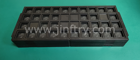
The picture is for reference only, please refer to the product specification
- EP3C55F484I7
- Intel
- IC FPGA 327 I/O 484FBGA
- Embedded - FPGAs (Field Programmable Gate Array)
- EP3C55F484I7 Datasheet
- 484-BGA
- 484-BGA
-
 Lead free / RoHS Compliant
 - 2973
- Spot Inventory / Athorized Dstributor / Factory Excess Stock
- 1 year quality assurance 》
- Click to get rates


What is EP3C55F484I7
Intel Part Number EP3C55F484I7(Embedded - FPGAs (Field Programmable Gate Array)), developed and manufactured by Intel, distributed globally by Jinftry. We distribute various electronic components from world-renowned brands and provide one-stop services, making us a trusted global electronic component distributor.
EP3C55F484I7 is one of the part numbers distributed by Jinftry, and you can learn about its specifications/configurations, package/case, Datasheet, and other information here. Electronic components are affected by supply and demand, and prices fluctuate frequently. If you have a demand, please do not hesitate to send us an RFQ or email us immediately [email protected] Please inquire about the real-time unit price, Data Code, Lead time, payment terms, and any other information you would like to know. We will do our best to provide you with a quotation and reply as soon as possible.
EP3C55F484I7 Specifications
- Part NumberEP3C55F484I7
- CategoryEmbedded - FPGAs (Field Programmable Gate Array)
- ManufacturerIntel
- DescriptionIC FPGA 327 I/O 484FBGA
- Package484-BGA
- SeriesCyclone® III
- Voltage - Supply1.15 V ~ 1.25 V
- Operating Temperature-40°C ~ 100°C (TJ)
- Mounting TypeSurface Mount
- Package / Case484-BGA
- Supplier Device Package484-FBGA (23x23)
- Number of I/O327
- Number of LABs/CLBs3491
- Number of Logic Elements/Cells55856
- Total RAM Bits2396160
Application of EP3C55F484I7
EP3C55F484I7 Datasheet
EP3C55F484I7 Datasheet , 484-BGA,Cyclone® III,1.15 V ~ 1.25 V,-40°C ~ 100°C (TJ),Surface Mount,484-BGA,484-FBGA (23x23),327,3491,55856,2396160
EP3C55F484I7 Classification
Embedded - FPGAs (Field Programmable Gate Array)
FAQ about Embedded - FPGAs (Field Programmable Gate Array)
-
1. What is the hardware of FPGA?
FPGA (Field-Programmable Gate Array) is a hardware device, not software. FPGA is a programmable hardware device consisting of a large number of logic units, storage units and interconnection resources, which can realize complex digital circuits and system designs.
The hardware structure of FPGA mainly includes the following parts:
Logic unit: FPGA contains programmable logic blocks that can perform logical and arithmetic operations.
Interconnection resources: These resources act as connections between logic blocks, allowing data to be transferred between different logic blocks.
Memory unit: Used to store configuration information and temporary data, supporting FPGA operations and logic processing.
The characteristics and application scenarios of FPGA include:
Programmability: FPGA can change the structure of its internal circuits by loading configuration information to achieve different functions.
High-speed execution: FPGA performs logic operations at the hardware level, which is usually several orders of magnitude faster than software execution.
Wide application: FPGA is widely used in many fields such as communications, medical, automotive, aerospace, industrial automation, etc. to implement complex digital circuits and algorithms, improve equipment performance, reduce power consumption or achieve specific functional requirements. -
2. Can FPGAs replace microcontrollers?
FPGAs cannot completely replace microcontrollers (MCUs). Although FPGAs and MCUs have their own characteristics and advantages in functions and applications, FPGAs cannot completely replace MCUs. There are significant differences between FPGAs and MCUs in terms of programmability, processing power, flexibility, development cycle, and cost.
The main differences between FPGAs and MCUs include:
Programmability: FPGAs are programmable and can be reprogrammed to achieve new functions, while MCUs are fixed and cannot be changed.
Processing power: FPGAs are usually used in high-performance computing, digital signal processing, image processing, and other fields, while MCUs are usually used for simple tasks such as controlling and monitoring equipment and sensors.
Flexibility: FPGA is more flexible than MCU and can be programmed and reprogrammed according to different applications, while MCU can usually only run predefined programs in its internal memory.
Development cycle: FPGA has a longer development cycle than MCU because FPGA needs to be designed, verified and debugged, while MCU usually only needs to write and debug programs.
Cost: FPGA costs more than MCU because FPGA needs to be manufactured and tested, and a lot of design and verification work is required, while MCU has a relatively low cost.
In specific application scenarios, FPGA and MCU each have their own advantages:
Advantages of FPGA: high programmability, parallel processing capability, high performance, suitable for applications that require rapid prototyping and system upgrades, suitable for scenarios with high real-time requirements.
Advantages of MCU: high integration, low cost, low power consumption, suitable for scenarios with strict power consumption requirements.
In summary, although FPGA performs well in some high-performance and flexible application scenarios, MCU still has irreplaceable advantages in simple control and monitoring tasks. -
3. Is FPGA analog or digital?
FPGAs are digital. FPGAs (field programmable gate arrays) are integrated chips that are mainly digital circuits, not analog. FPGAs are a type of programmable logic device that processes digital signals instead of analog signals.
FPGAs are a type of programmable logic device, a type of programmable logic device (PLD). It solves the shortcomings of traditional custom circuits, while also overcoming the shortcomings of the limited number of gate circuits in the original programmable devices. FPGA is a product that is further developed on the basis of traditional logic circuits and gate arrays such as PAL (Programmable Logic Array), GAL (General Array Logic), and CPLD (Complex Programmable Logic Device).
The design process of FPGA includes the use of computer-aided design, by drawing schematic diagrams that implement user requirements, editing Boolean equations, or using hardware description languages as design inputs. Then after a series of conversion programs, automatic layout and routing, and simulation processes, the FPGA data file is finally generated to initialize the FPGA device.
We are a professional PCB manufacturer who offers comprehensive PCB manufacturing services including: professional Ceramic PCB HDI PCB Heavy Copper PCB High-TG PCB High Speed PCB High Frequency PCB Metal Core PCB PCB fabrication and PCB assembly, providing fast turnaround prototypes for high-end products.


• Prompt Responsiveness
• Guaranteed Quality
• Global Access
• Competitive Market Price
• One-Stop support services of supply chain
Jinftry, Your most trustworthy component supplier, welcome to send us the inquiry, thank you!
Do you have any questions about EP3C55F484I7 ?
Feel free to contact us: