Power Integrity (PI) Design and Test Methodology
Power Integrity (PI) Design and Test Methodology
Power integrity (Power Integrity, referred to as PI) is a very important part of electronic system design, especially high-speed digital systems.
PI is generally concerned with ensuring that the various components in the system receive clear, clean, and constant power.
To this end, a suitable power distribution network (Power Distribution Network, PDN) needs to be designed and tested to ensure that its performance is up to standard.
The following are design and test methods for power integrity:
1. Design method:
PDN design: The PDN includes all the connection elements from the power source (such as a power converter) to the load of the chip or device.
Examples of power converters are:ACT30AHT ,ACT334US-T,ALTAIR04-900TR,AP3103AKTR-G1 ,AP3772AK6TR-G1-2,AP39303S16-13 。。
Decoupling Capacitor Selection: These capacitors reduce power supply noise. Selecting the proper capacitor value and type is critical to meeting the target impedance.
Planar Design: Use continuous power and ground planes to reduce power supply noise. The distance, size, and relative position between planes all affect the performance of the PDN.
VRM/Power Converter Selection: Make sure to select the proper power converter to meet the design requirements.
Simulation and Modeling: Use PI simulation tools (such as ANSYS SIwave, Keysight ADS, Cadence Sigrity, etc.) to predict the performance of the PDN.
How to Design for Power Integrity
2. Test method:
Time Domain Reflectometry/Transmission Testing (TDR/TDT): Can determine the impedance characteristics of the PDN and pinpoint problem areas.
Power supply noise measurements: Use oscilloscopes and probes to measure noise and interference on power supplies.
Frequency domain test: Use a network analyzer to perform S-parameter measurements to analyze the performance of the PDN in the frequency domain.
Thermal testing: Check the performance of the PDN at different temperatures.
VRM/power converter performance testing: Verify that the converter meets design requirements such as output ripple, efficiency, load and line regulation, etc.
Actual working environment test: run the device in a real working environment to observe whether there are power problems or other related problems.
To ensure power integrity, signal integrity (SI) and electromagnetic compatibility (EMC/EMI) usually also need to be considered.
These three are usually interrelated in high-speed digital system design and need to be considered comprehensively.
Trends and challenges in power supply design:

Chip process technology DDR rate DDR interface voltage current
Power requirements:
The Tolerace of chip power supply to voltage is generally 5% or 3%, or even 1%

The power requirement of 15mv or even 10mv poses great challenges to testing and design

Why does the power supply have ripple noise?
- When the chip is working, the regulated power supply module VRM senses the change of its output voltage and adjusts its output current, thereby adjusting the output voltage back to the rated output value
-Unable to respond in real time to the rapid change of the chip's current demand, the power supply voltage drops, resulting in power supply noise
•Current chips are working faster and faster, high-frequency transient currents are getting bigger and bigger, and the noise brought by them cannot be ignored more and more;
Synchronous switching noise from high frequency noise sources:
Synchronous switching noise is referred to as SSN, which refers to the
The instantaneous change of current when the chip is in the switching state
(di/dt), inductance in the return path
When the AC voltage drop is formed, causing noise,
Also called Δi noise;
Sources of Ripple Noise:
• Noise: simultaneous switching noise SSN, etc.
• Ripple: line frequency and switching frequency and frequency multiplication
• Interference: interference of surrounding signals or load mutation, etc.
Power Distribution Network (PDN)
"Power cord" turned into "power distribution network (PDN)";
-PDN includes VRM, board-level capacitors (electrolytic capacitors/tantalum capacitors/ceramic capacitors), planar capacitors, chip parasitic parameters, PKG capacitors, Die capacitors, etc.;
• PDN design is completed by power module, board-level hardware, and chip design;
Switching power supply (DC/DC) and linear power supply (LDO)
-DC/DC: through the switch, control the PWM duty cycle to obtain the output voltage
-LDO: Consume part of the energy through heat to achieve step-down
Total inductance of capacitors behind the board
.In addition to the parasitic inductance of the capacitor itself, there will be installation parasitic inductance, plane parasitic inductance and via parasitic inductance when installed on a single board.
. The total parasitic inductance causes the resonant frequency to drop
. The optimization of PI layout is to minimize these parasitic inductance

Plane capacitance:
Planar capacitance: the capacitance value is mainly determined by the size of the plane, the distance between the planes, and the dielectric coefficient of the material;
80*8r*W*1
C = ------------------------
h
Where SO = permittivity of free space = 0.225pf/inch
Sr = relative permittivity (dielectric constant) of the dielectric material
W = width of the power plane in inches
I = length of the power plane in inches
h = distance between the power/ground plane in inches

Improvement method of DC voltage drop
10 JULY 2020 13• High density/low cost/high current etc.
The problem of causing DC voltage drop is clear
Significantly increased; • Increasing the output voltage value of the power supply can
partially solve the problem; or
Feedback line to reduce DC voltage drop
PI Design----Target Impedance
Target impedance: meet the maximum transient current change of the load, and the voltage fluctuation range is within the allowable range of the chip. The maximum value of the PDN’s own impedance is allowed. If this impedance value is exceeded, the power supply fluctuation may exceed the voltage allowable range. The target impedance design method is A conservative approach to design;
• 1V voltage, 5% voltage fluctuation requirement, maximum transient current 5A
• Ztarget=1*0.05/5=10m Euro

PI design - the realization of the target impedance
• Select a good VRM • Filter capacitor • Stack design • Layout • Satisfy Ztarget in the frequency range of interest
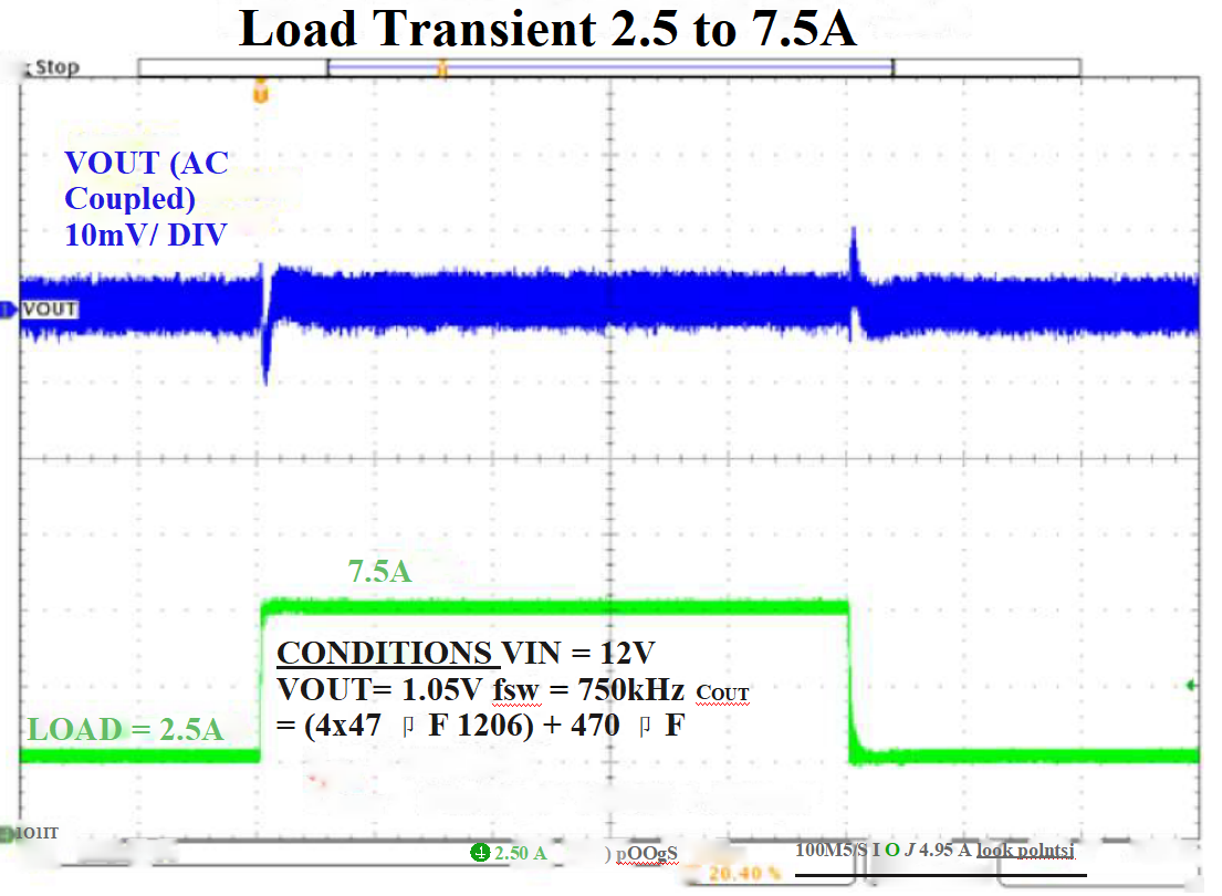
Requirements for high-speed single-board PI testing
10 JULY 2020 21• High precision: small noise test 10mv or less
• High bandwidth: the switching frequency and rise time of the switching power supply become faster & the high-speed transient current of the chip • DC coupling: energy saving and environmental protection, DVFS dynamic voltage frequency adjustment
• Input impedance: DC high impedance, AC 50 ohm
• Abundant test connection methods and standard test software
• Combined analysis of time domain and frequency domain
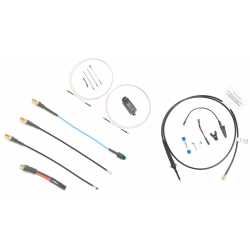
Rich connection methods
30MMCX interface
SMA interface
U.FL interface
Welding interface
SQ-PIN interface
Point measurement
Capacitor clip CLAMP

PI test other points for attention
10 JULY 2020 31• No matter what kind of test connection, try to minimize the test loop (short ground wire as possible)• Recommend Bottom surface test to reduce the introduction of interference
• The test point should be as close as possible to the power supply pin of the chip
• Power supply ripple noise test is a stress test under maximum load
edit author:
![]()
Jinftry(Hong Kong registered company name: JING FU CAI (HONGKONG) INTERNATIONAL CO., LIMITED) was established in 2013, headquartered in Hong Kong, China, with a branch in Shenzhen, China. It is a global supplier of electronic components and a well-known and competitive electronic product distributor in Asia. Is also an excellent strategic partner of global ODM/OEM/EMS, able to quickly find authentic and traceable electronic components for customers to purchase.


